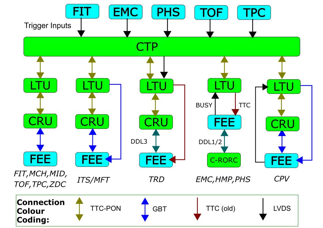
A Large Ion Collider Experiment (ALICE) has been conceived and constructed as a heavy-ion experiment at the LHC. During LHC Runs 1 and 2, it has produced a wide range of physics results using all collision systems available at the LHC. In order to best exploit new physics opportunities opening up with the upgraded LHC and new detector technologies, the experiment has undergone a major upgrade during the LHC Long Shutdown 2 (2019-2022). This comprises the move to continuous readout, the complete overhaul of core detectors, as well as a new online event processing farm with a redesigned online-offline software framework. These improvements will allow to record Pb-Pb collisions at rates up to 50 kHz, while ensuring sensitivity for signals without a triggerable signature.
JINST 19 (2024) P05062
e-Print: arXiv:2302.01238 | PDF | inSPIRE
CERN-EP-2023-009
Figure group
Figure 3
Time frame and heartbeat frame structure in continuous and triggered mode. HeartBeat (HB) triggers are issued in continuous and triggered modes to all upgraded detectors. Physics triggers can be sent to upgraded detectors in triggered mode and are sent to non-upgraded detectors in all modes. HBF and TF rates are programmable with the following nominal values; HBF: 1 every orbit, $\sim$89.4 µs/$\sim$10 kHz, TF: 1 TF every 128 HBFs/$\sim$11 ms/$\sim$100 Hz. | 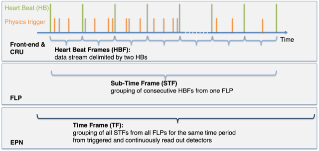 |

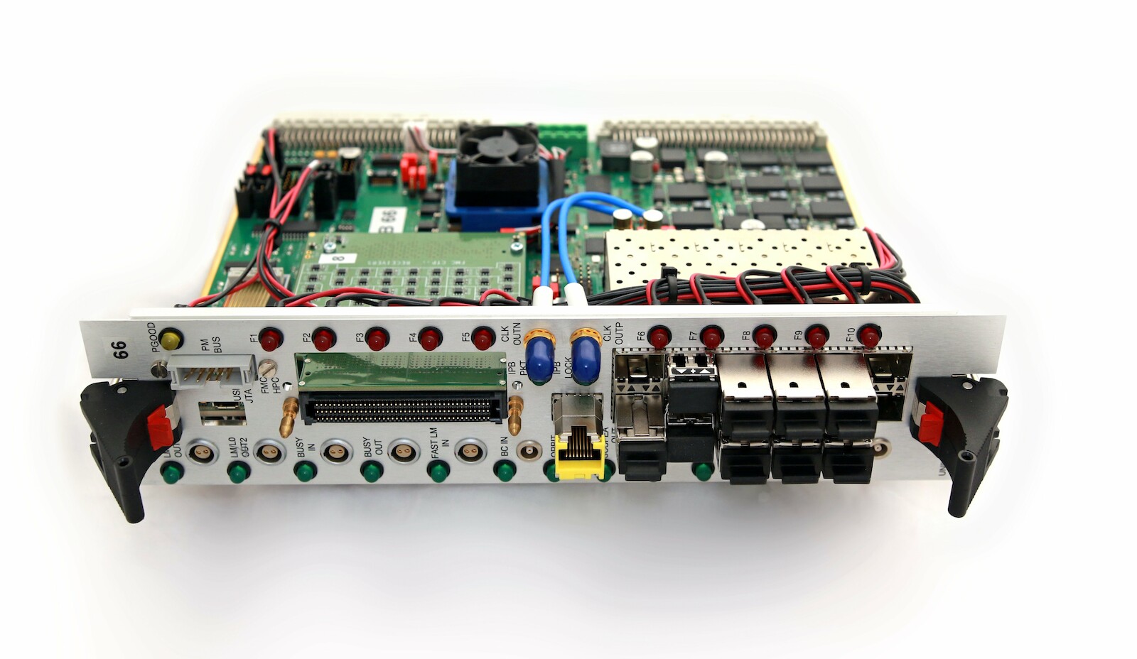
Figure 6
Picture of a CRU; bottom left, FPGA cooling radiator, bottom right, power mezzanine; top row; 3 out of 8 Minipods installed; top left, fiber optics cable to MPO connector on front panel; bottom left, SFP transceivers. | 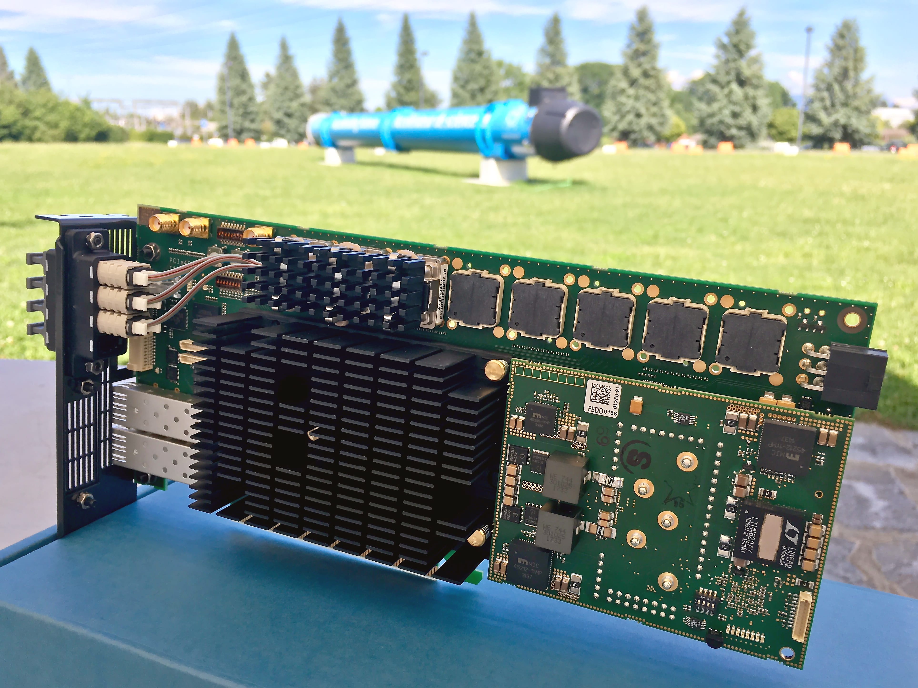 |
Figure 11
ALPIDE sensor chip detection efficiency and fake-hit rate vs global threshold setting. Beam test results (\SI{6}{\giga eV/\it{c}} pions, orthogonal incidence). ALPIDE substrate reverse bias: \SI{-3}{\volt}. |  |
Figure 12
ALPIDE chip hit-position resolution and average cluster size as a function of global threshold setting. Beam test results with \SI{6}{\giga eV/\it{c}} pions with perpendicular incidence. ALPIDE substrate reverse bias: ${\rm -3 V}$. | 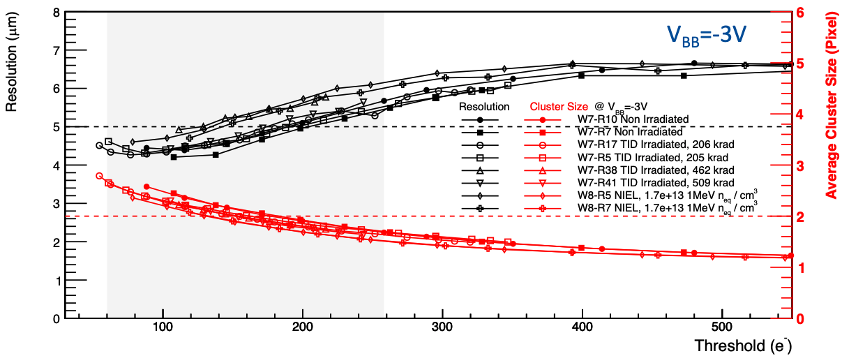 |
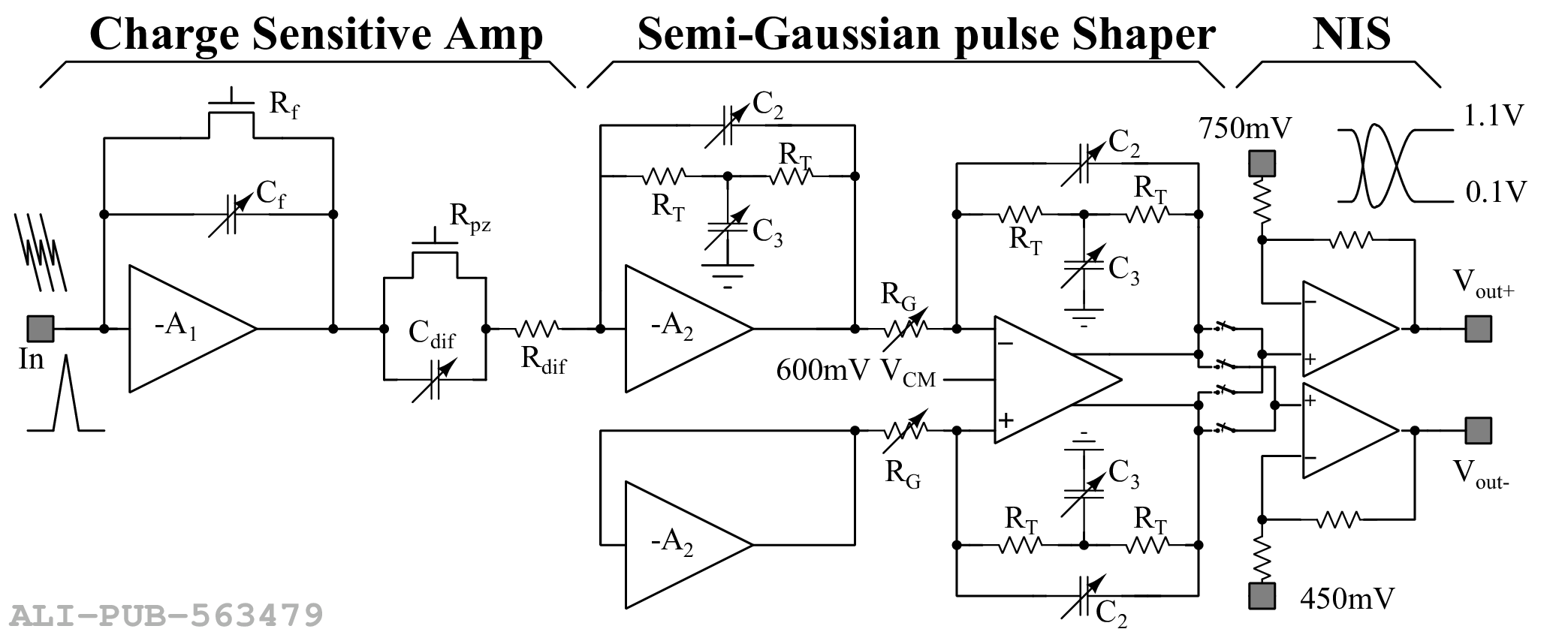

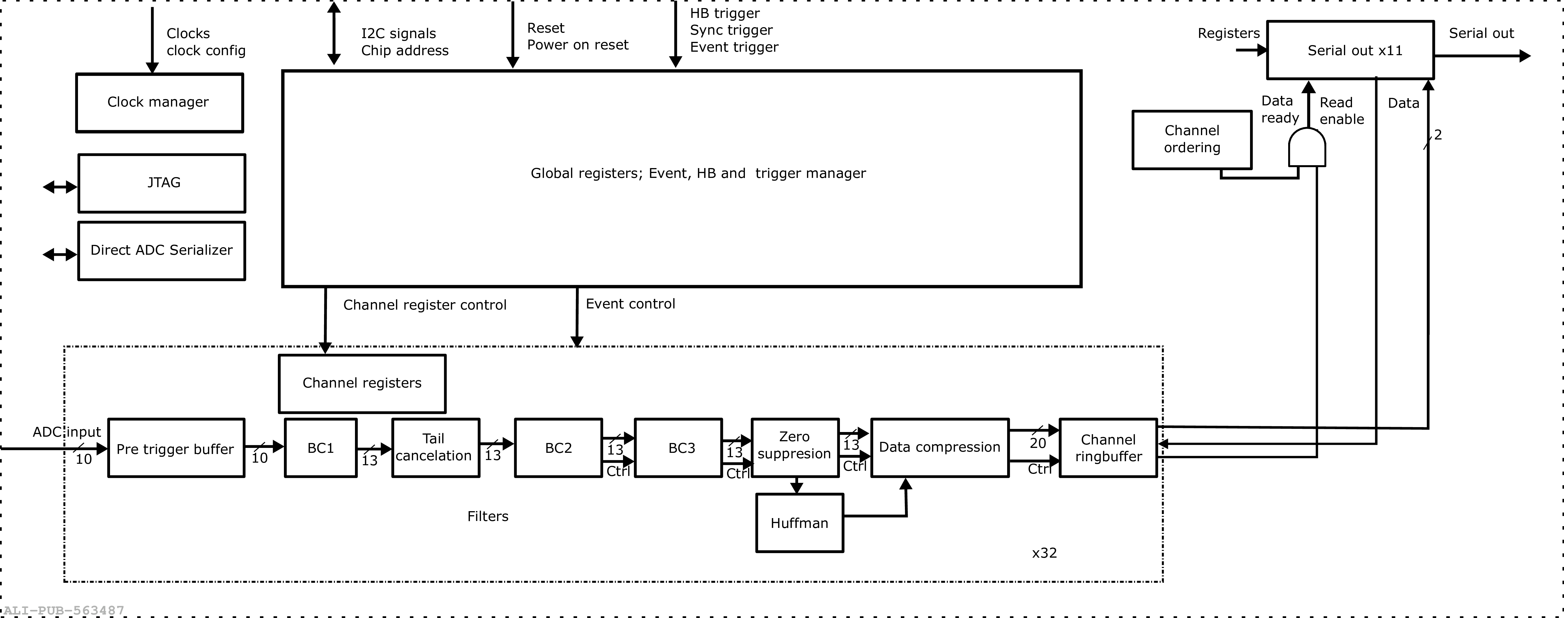
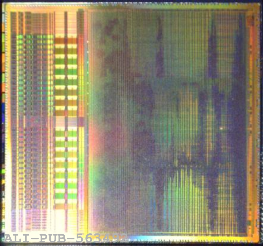
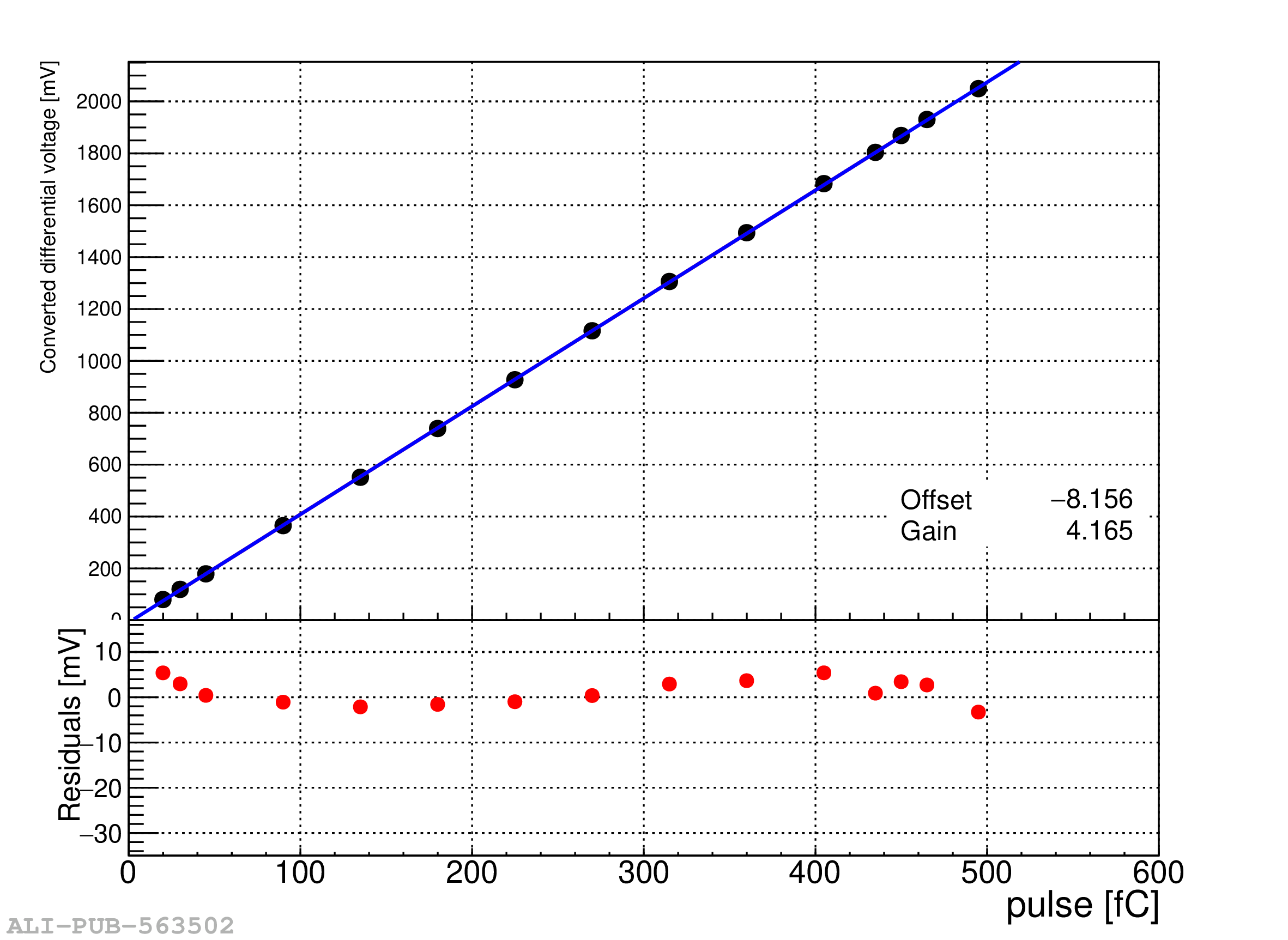

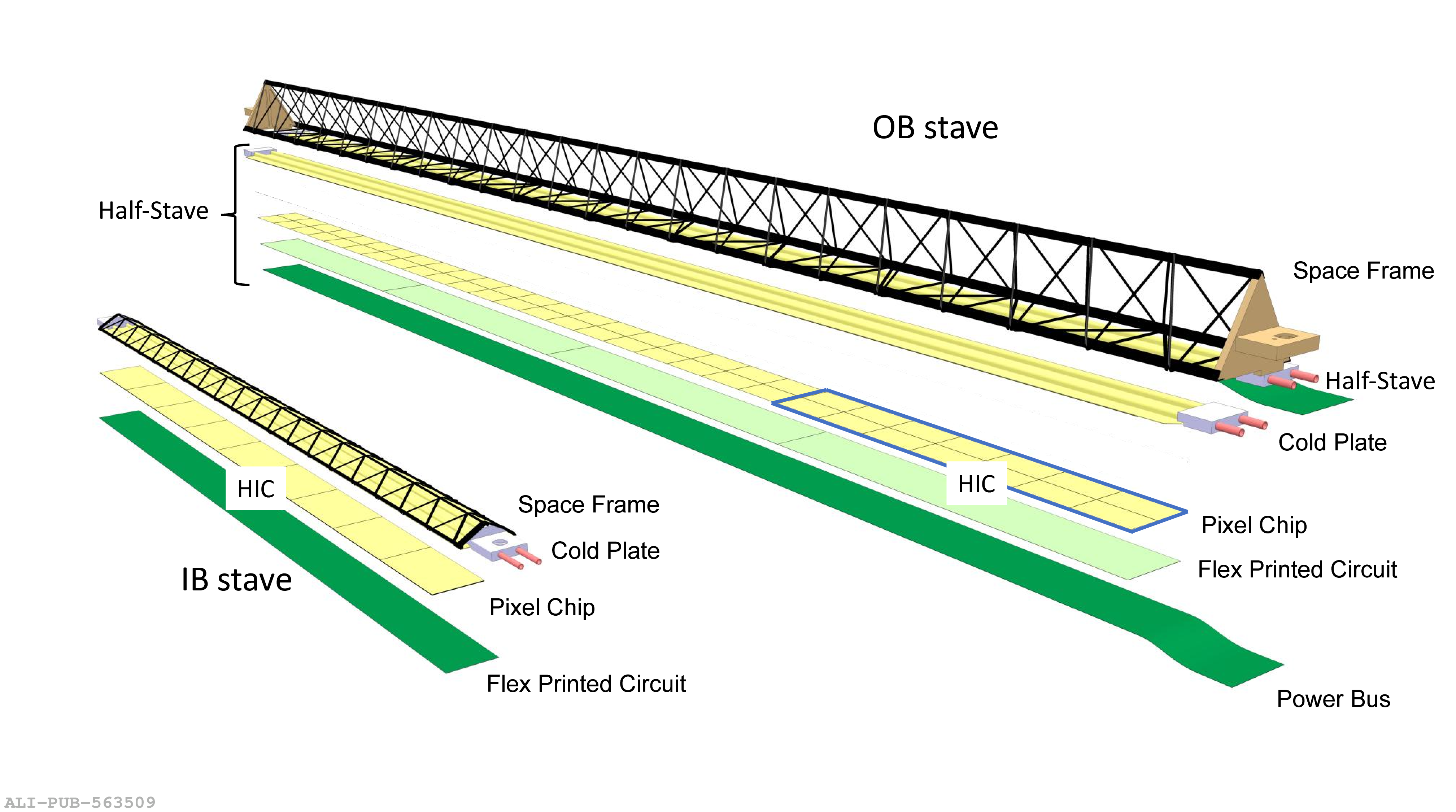
Figure 21
Inner HIC seen from the sensor side. The green tabs are used for fixing and handling, and are removed before mounting the HIC. | 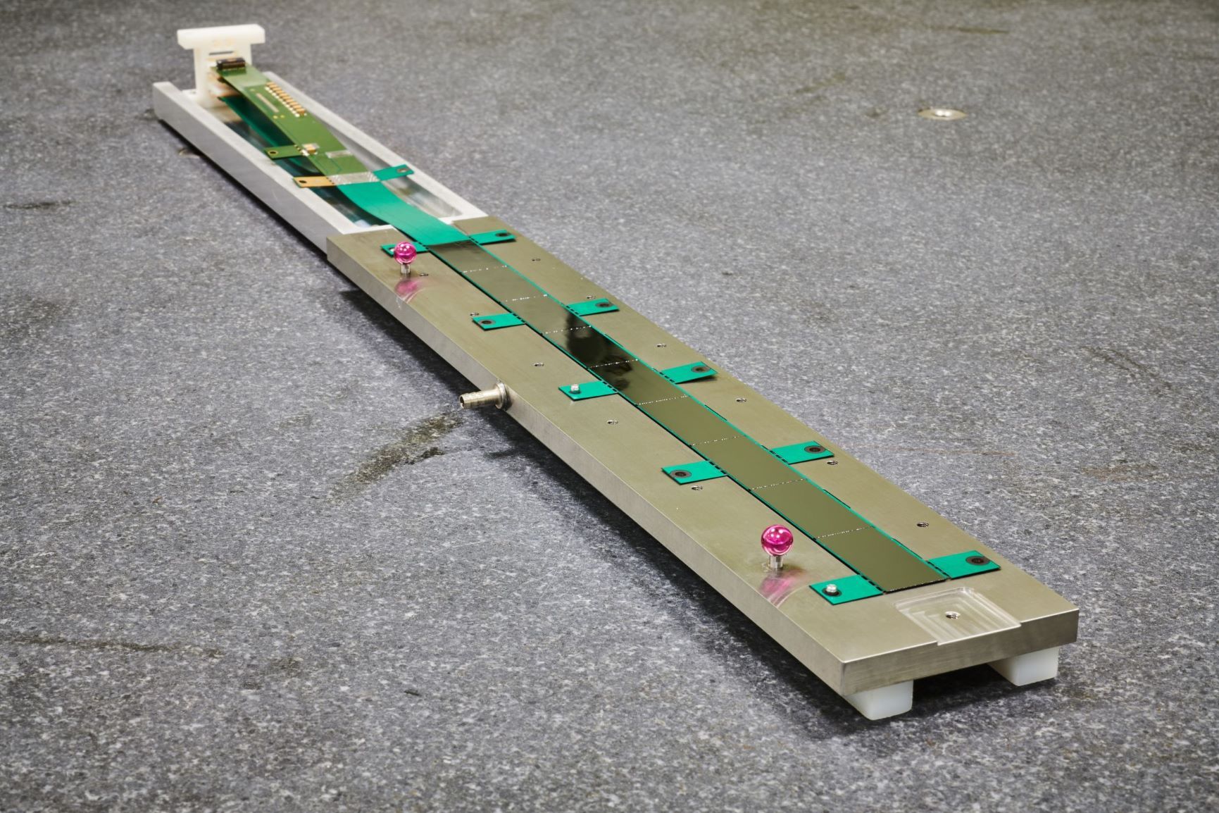 |


Figure 24
Space frame and cold plate cooling scheme (Left) Inner Barrel; (Right) Outer Barrel. | 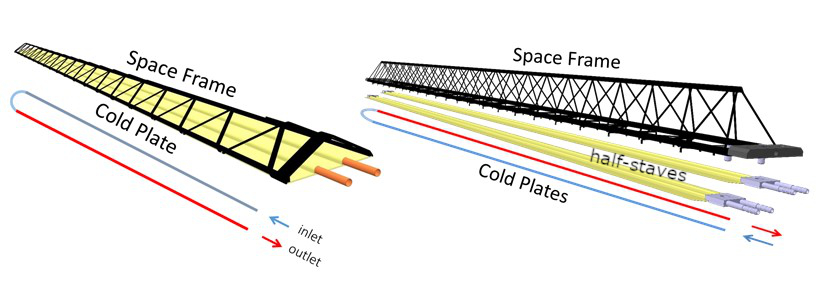 |


Figure 29
ITS2 in the clean room during on-surface commissioning. The lower left shows a zoomed-in view of the half barrels of the outer barrel (OB) and inner barrel (IB) type. | 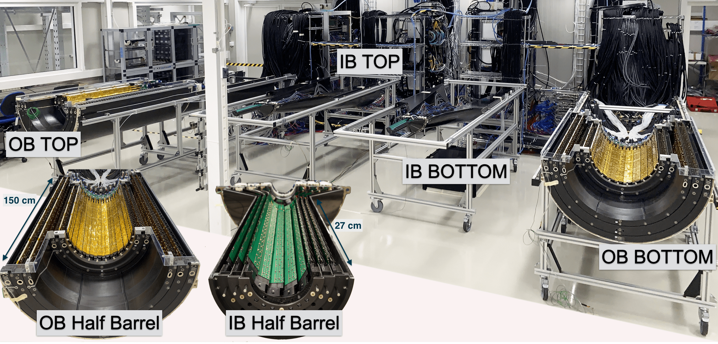 |
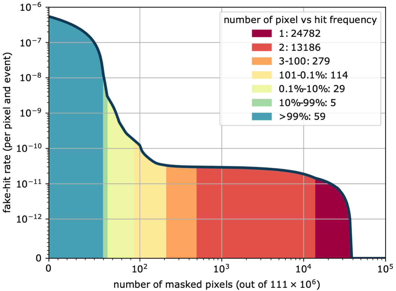
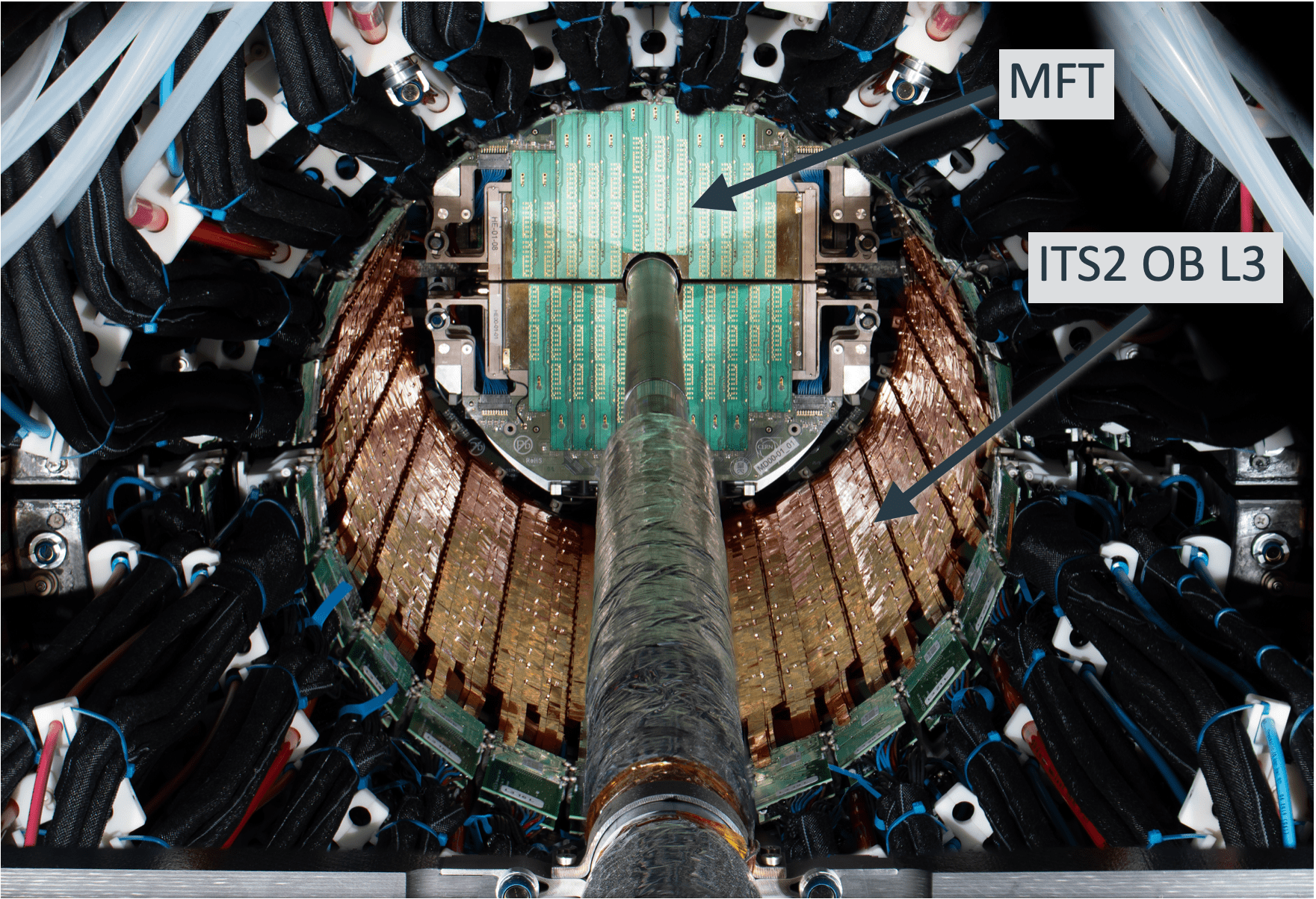
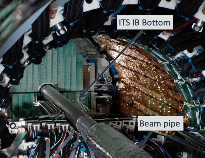
Figure 32
Event display of a cosmic muon traversing all layers of ITS2 twice, no magnetic field. |  |
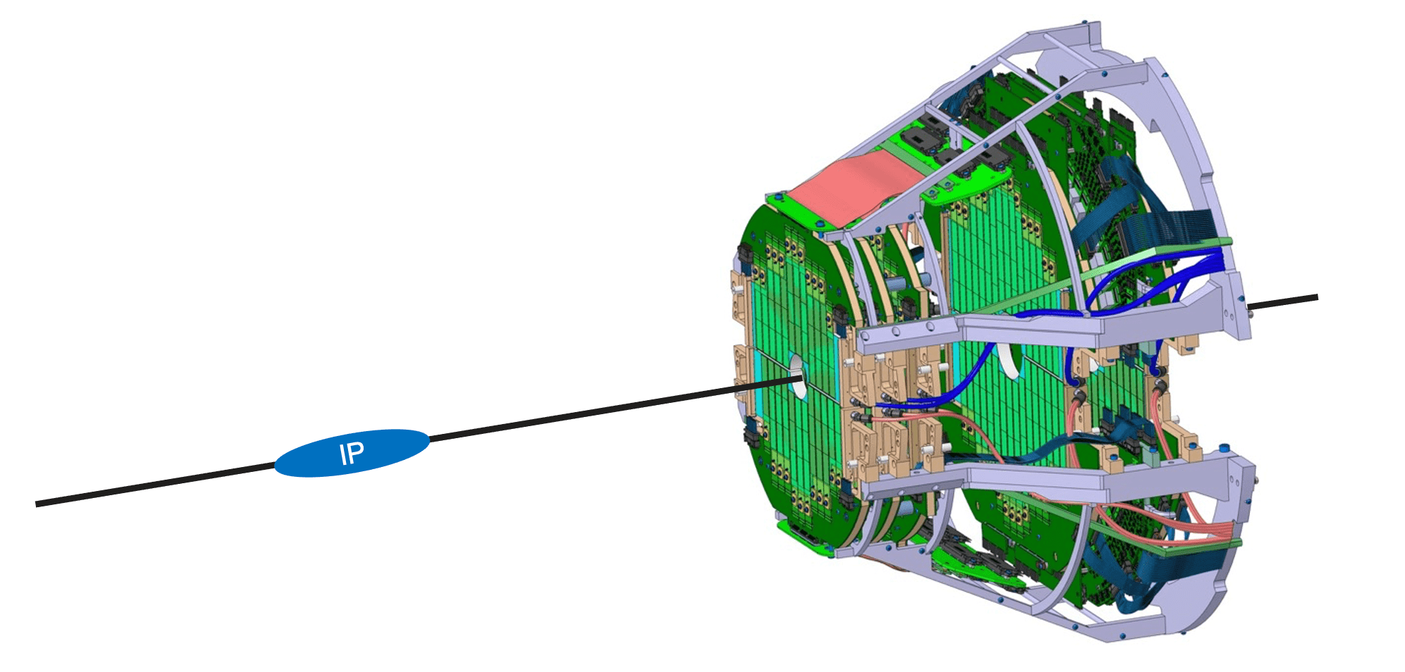
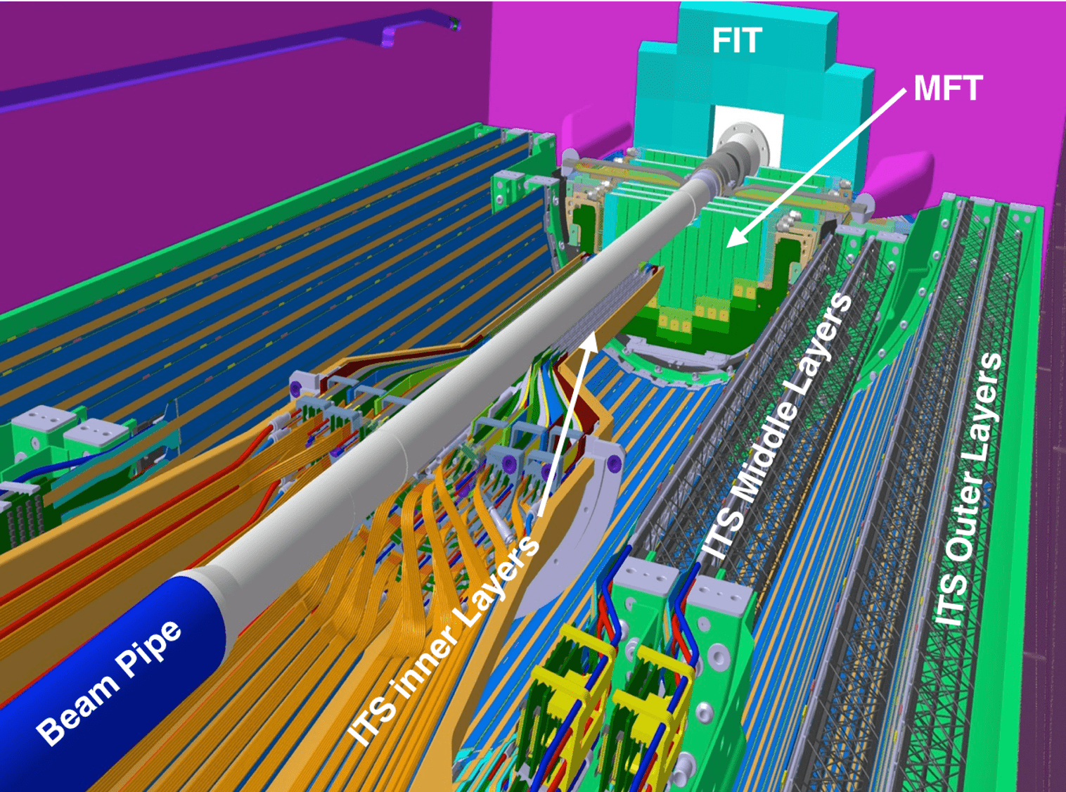
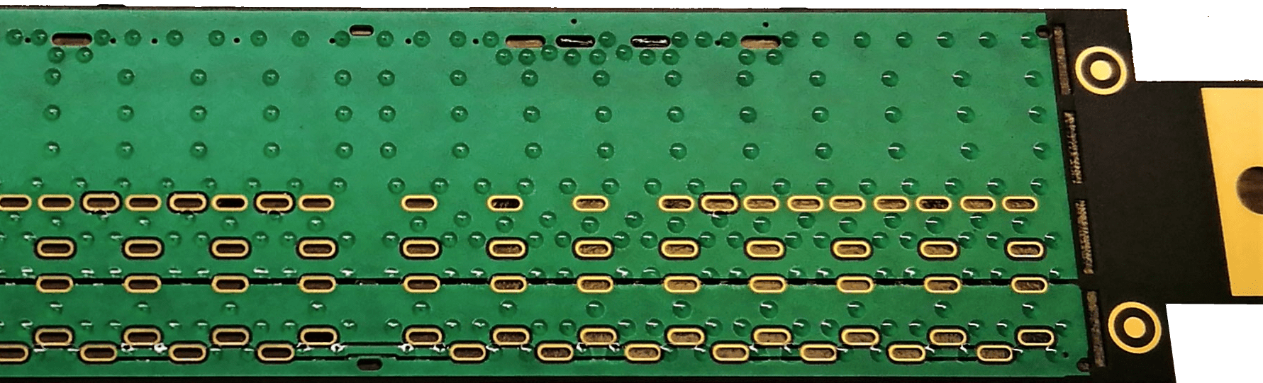

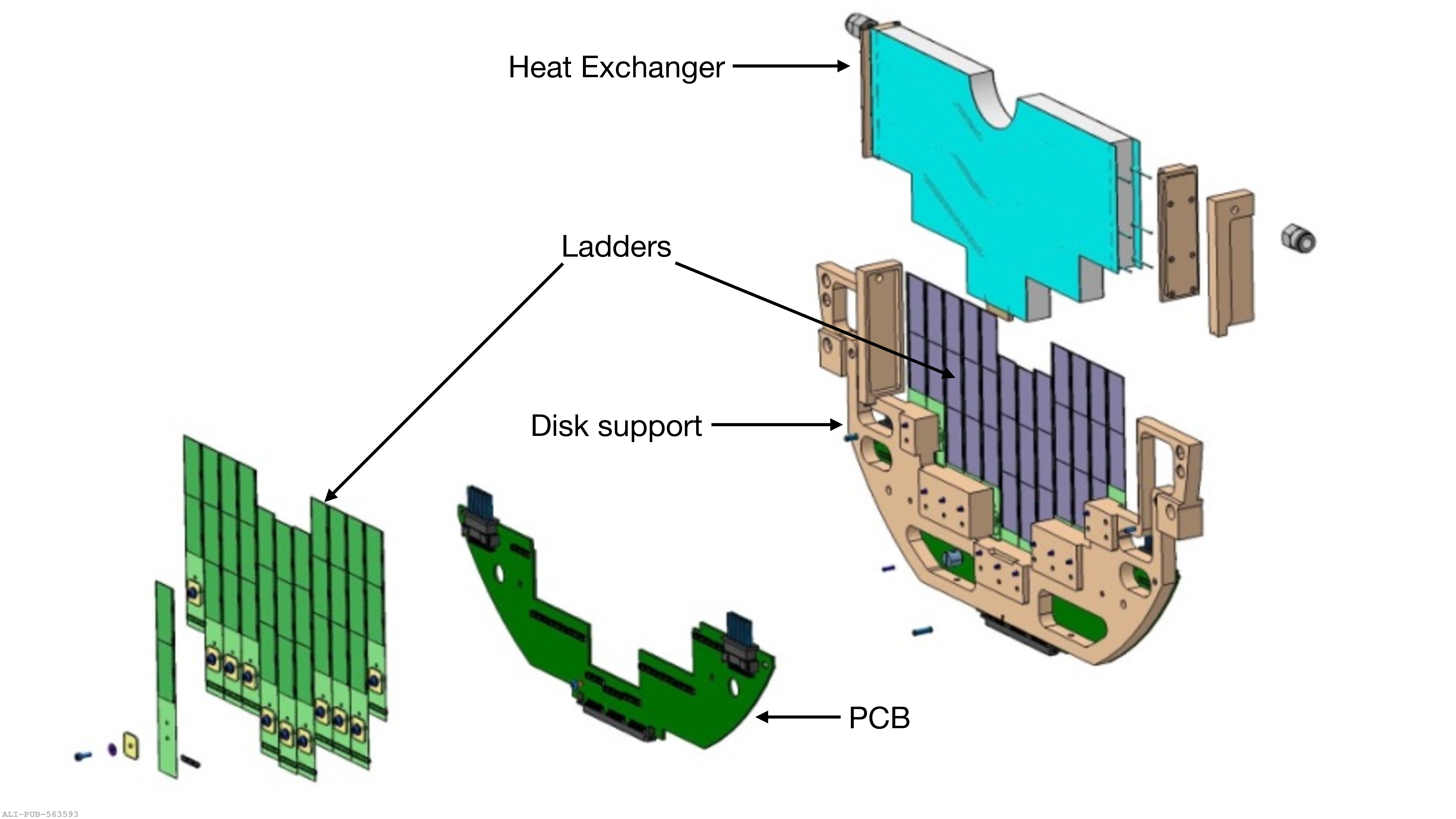
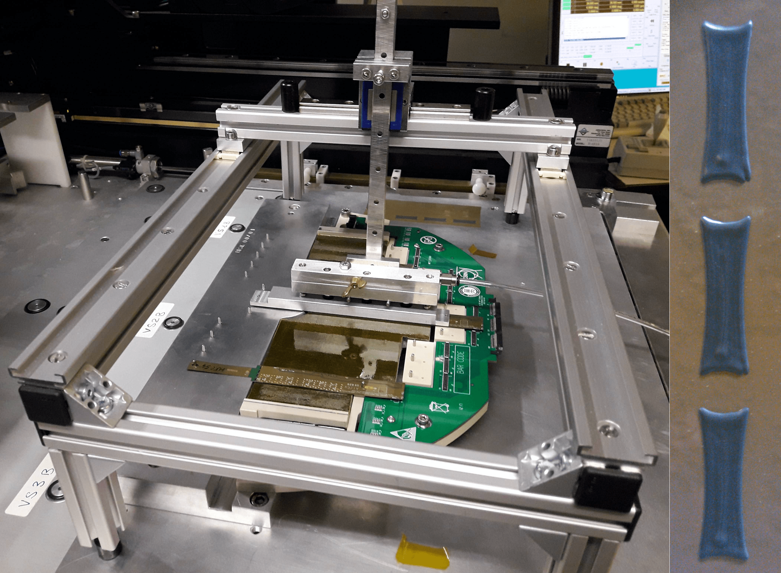

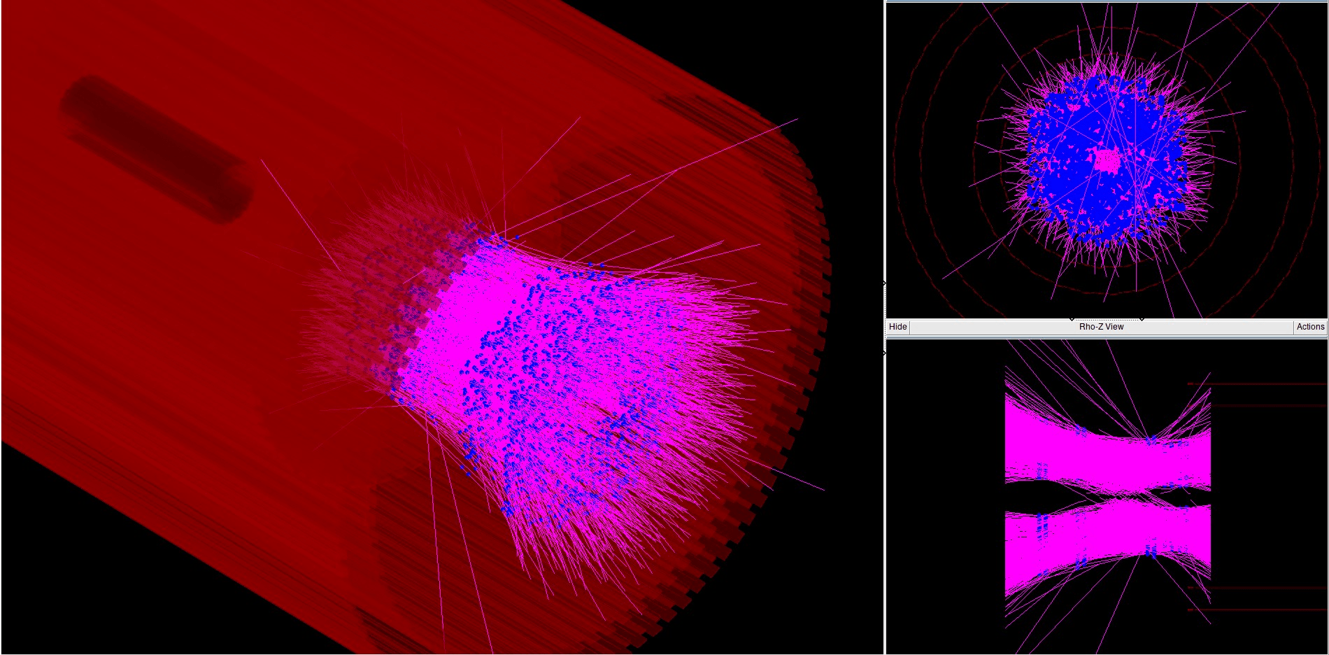
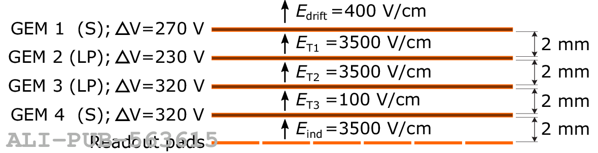
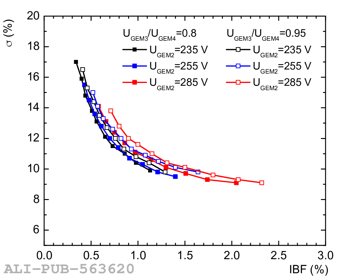

Figure 48
Detailed powering scheme of a GEM stack Each subsequent high-voltage channel is stacked on top of the lower-lying channel The ground reference is defined by a separate line connected to the ground of the detector The line for GEM\,4 top is shunted with a resistor ($R_{\text{shunt}}$) inside the high-definition current meter Each line is connected to the detector through a decoupling resistor ($R_{\text{dec}}$) The signal from a calibration pulser is coupled via a capacitor ($C_{\text{pulser}}$) to the line for GEM\,4 bottom Individual loading resistors ($R_{\text{load}}$) are mounted on all segments on the top sides of the GEMs Figure taken from . |  |
Figure 49
Schematic view of the TPC readout system Five SAMPA chips amplify, shape, and digitize the current signals picked up on the connected pads Two GBTx ASICs multiplex the digitized data GBTx\,0 forwards the data from two and a half SAMPA chips to a VTRx GBTx\,1 forwards the data from the other two and a half SAMPAs to one VTTx module (two optical transmit channels) GBTx\,0 also receives configuration data and the reference clock through the VTRx The reference clock is distributed to the other components A GBT-SCA chip is used for monitoring and configuration Figure taken from . | 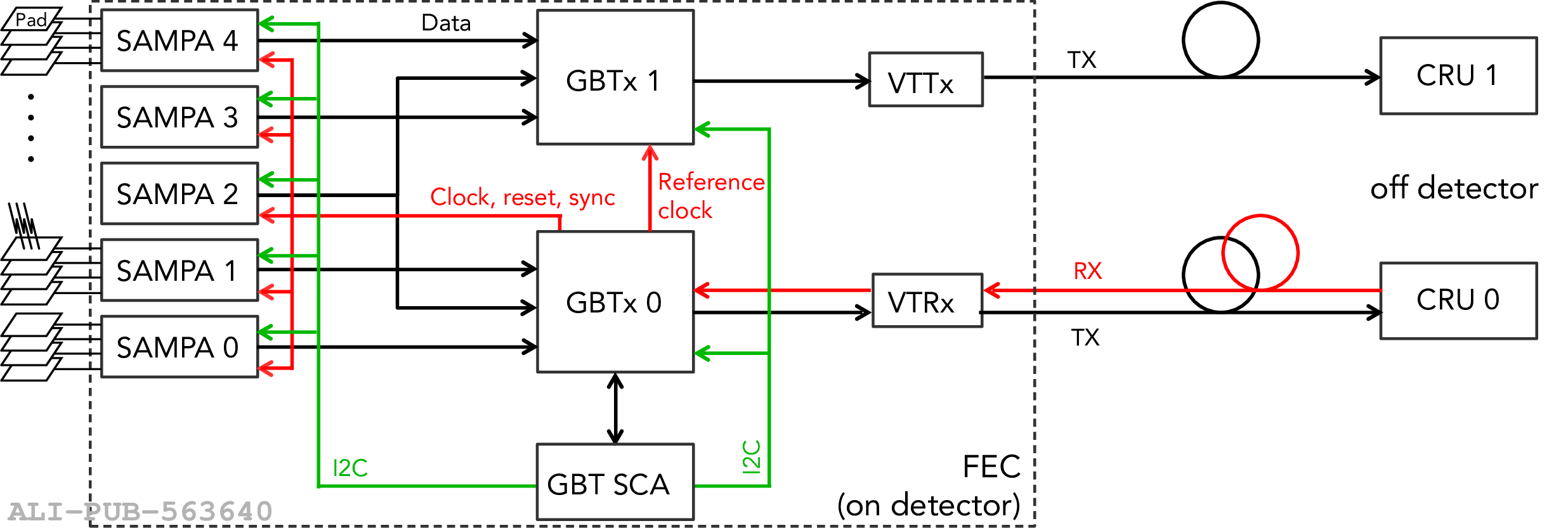 |
Figure 50
Layout of the final TPC FEC PCB Rev.\,1a The components are mounted on both sides of the board The figure shows the top side with five SAMPAs, two GBTx, one GBT-SCA, one VTRx, one VTTx and some other components On the bottom side a few additional small components and the connectors to the detector are placed. Figure taken from . | 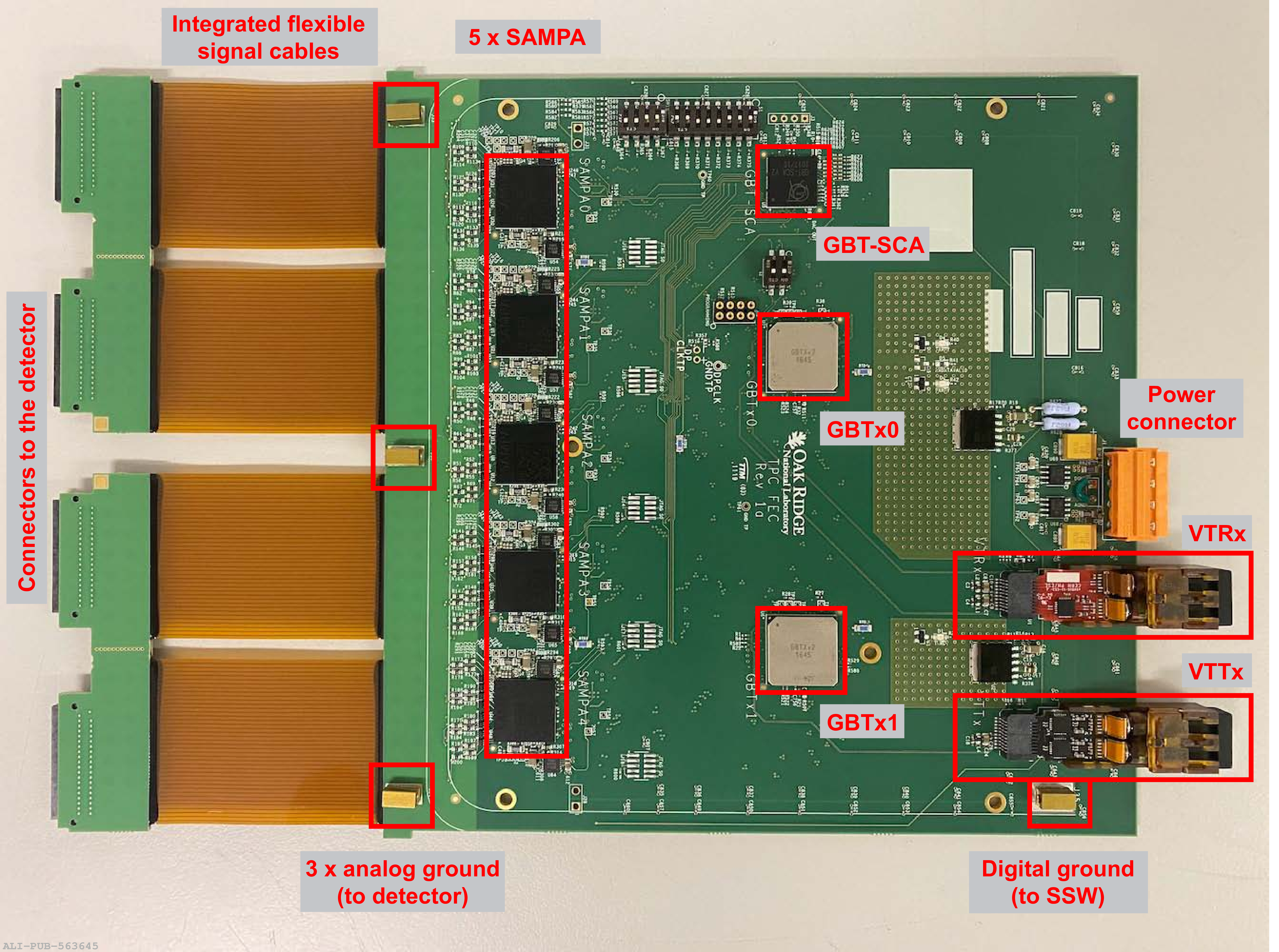 |
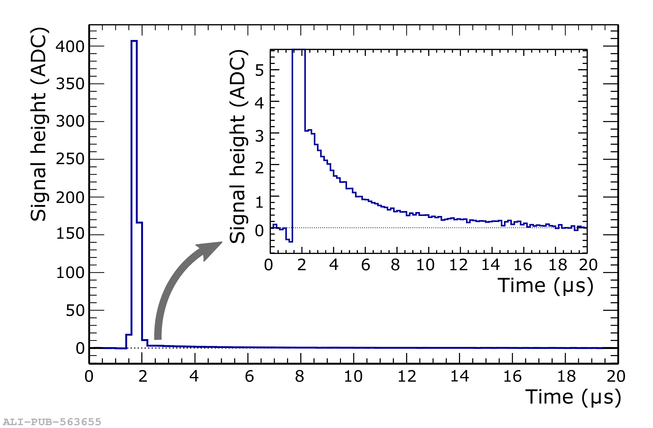
Figure 53
Visualization of the ion tailand of the common-mode effect for one readout channel zoomed around the baseline region The data are from a simulation with 30\% pad occupancy and without noise from theelectronics The common-mode effect shifts the baseline to below zero. The ion tail is visible forsignals with large amplitude Both effects are corrected in the CRU FPGAs. |  |
Figure 54
View of the FIT detectors illustrating the relative sizes of each component. From left to right FDD-A, FT0-A, FV0, FT0-C, and FDD-C are shown. Note that FT0-A and FV0 have a common mechanical support. FT0-A is the small quadrangular structure in the centre of the large, circular FV0 support. Note that all detectors are planar with the exception of FT0-C, which has a concave shape centered on the IP. The inset table lists the distance from the interaction point and the pseudorapidity coverage for each component. | 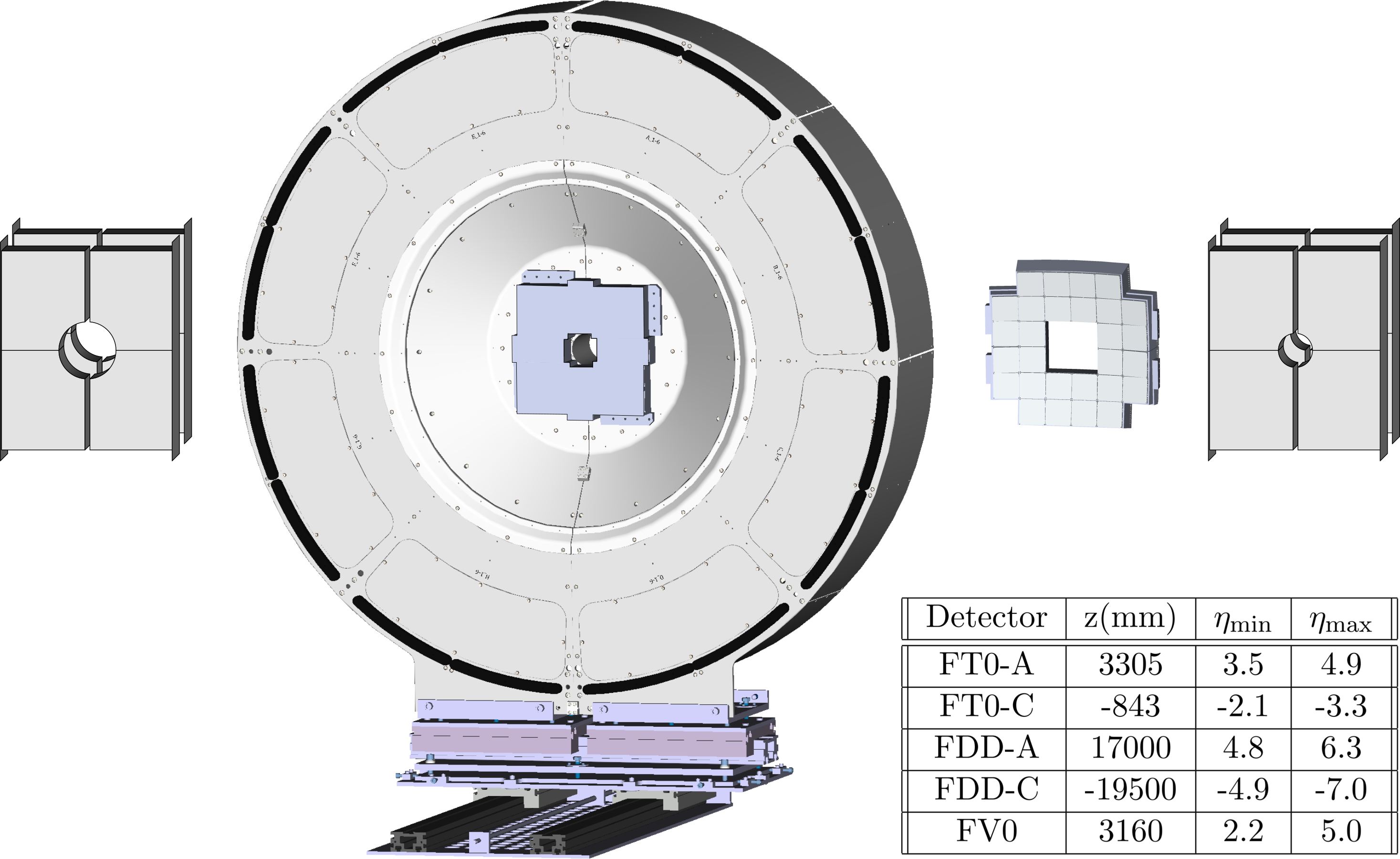 |
Figure 55
Photograph of one half of the FV0. The optical fibers connect the scintillators to the PMTs on the rim of the support structure, the black structure seen here. The center wall has been removed to show the scintillator, the surface matrix structure, and the optical fibers. | 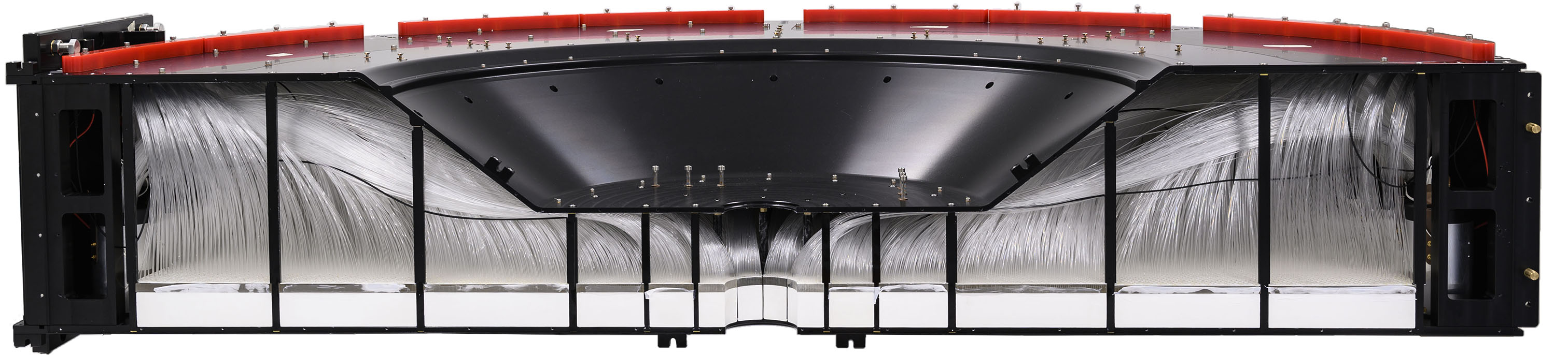 |
Figure 56
Schematic diagram of the FIT readout electronics. The MicroChannel Plates (MCP) are described in the FT0 section. |  |

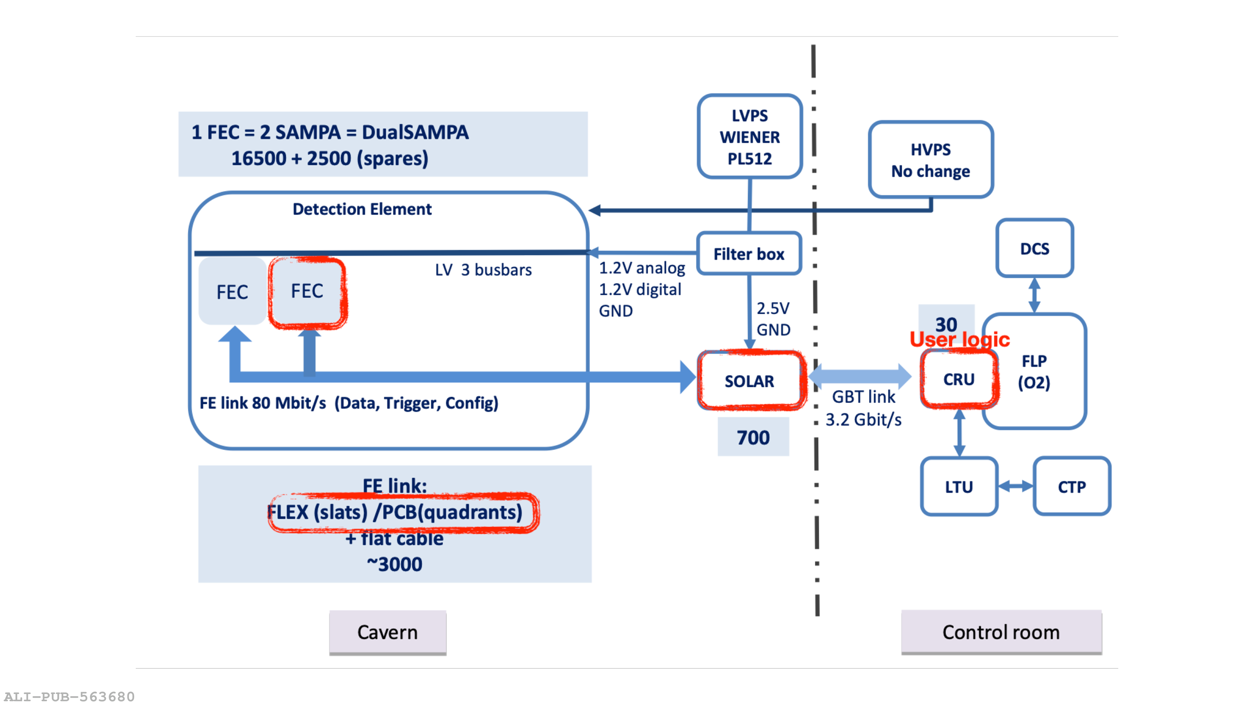

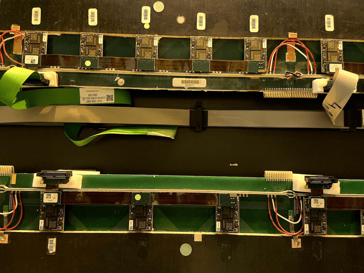

Figure 62
The SOLAR board: functional diagram (left panel) and photo of the board itself (right). | 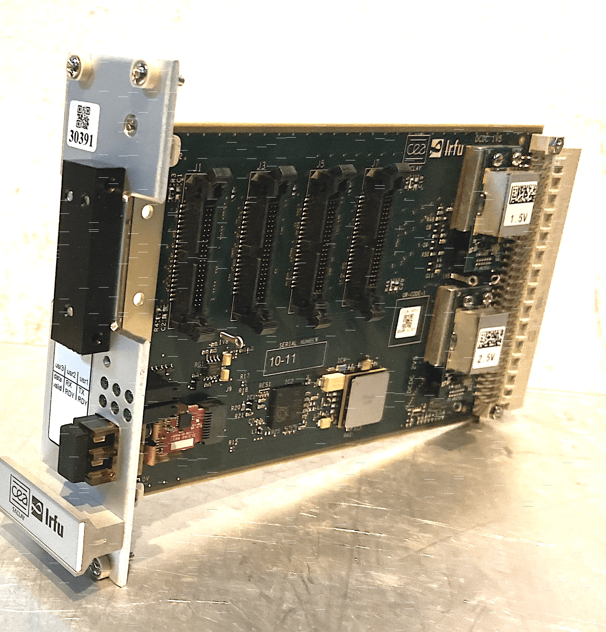 |

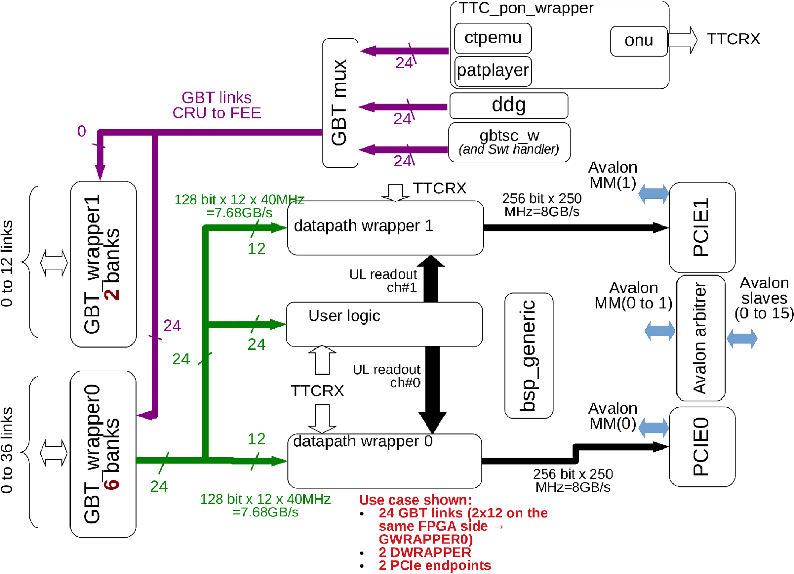


Figure 67
Wireless threshold distribution scheme (left) and master or node electronics card (right). | 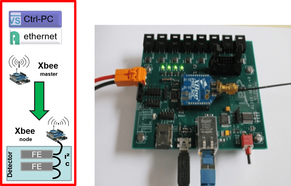 |
Figure 68
MID readout architecture (left) and readout cards (right picture) with local (LOC) (top right), regional (REG) (top left) and J2 bus (bottom) between local and regional. | 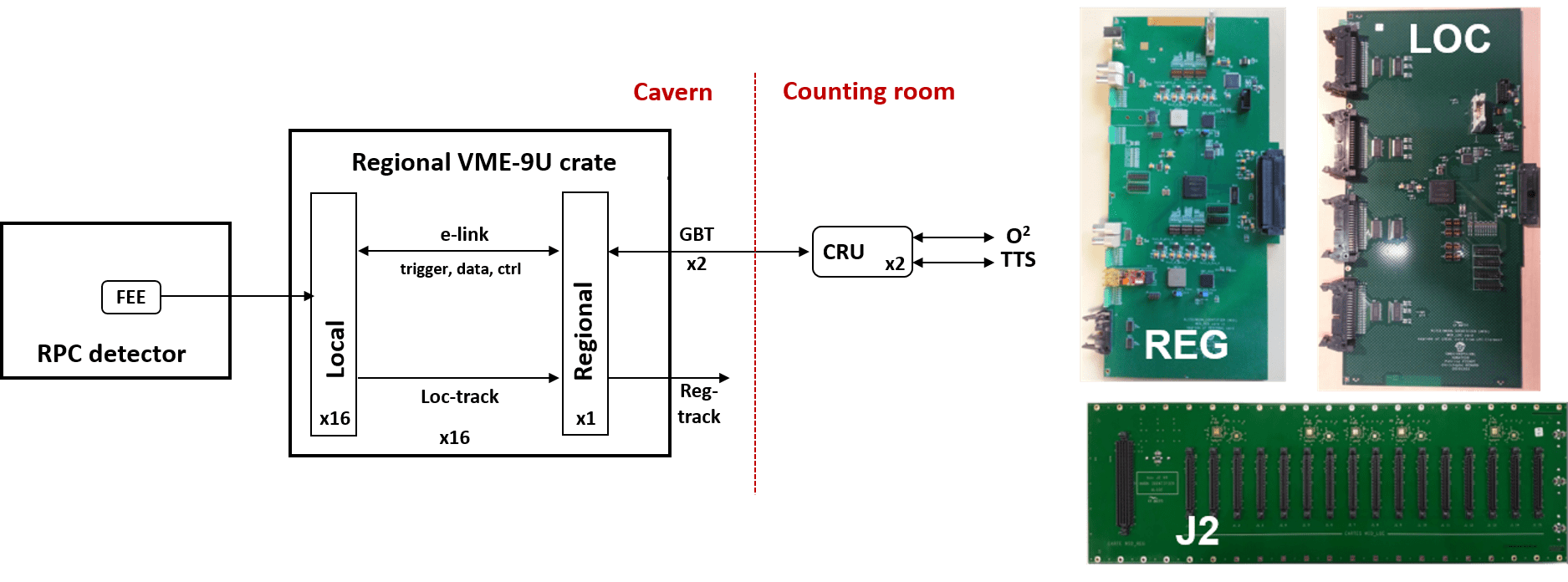 |
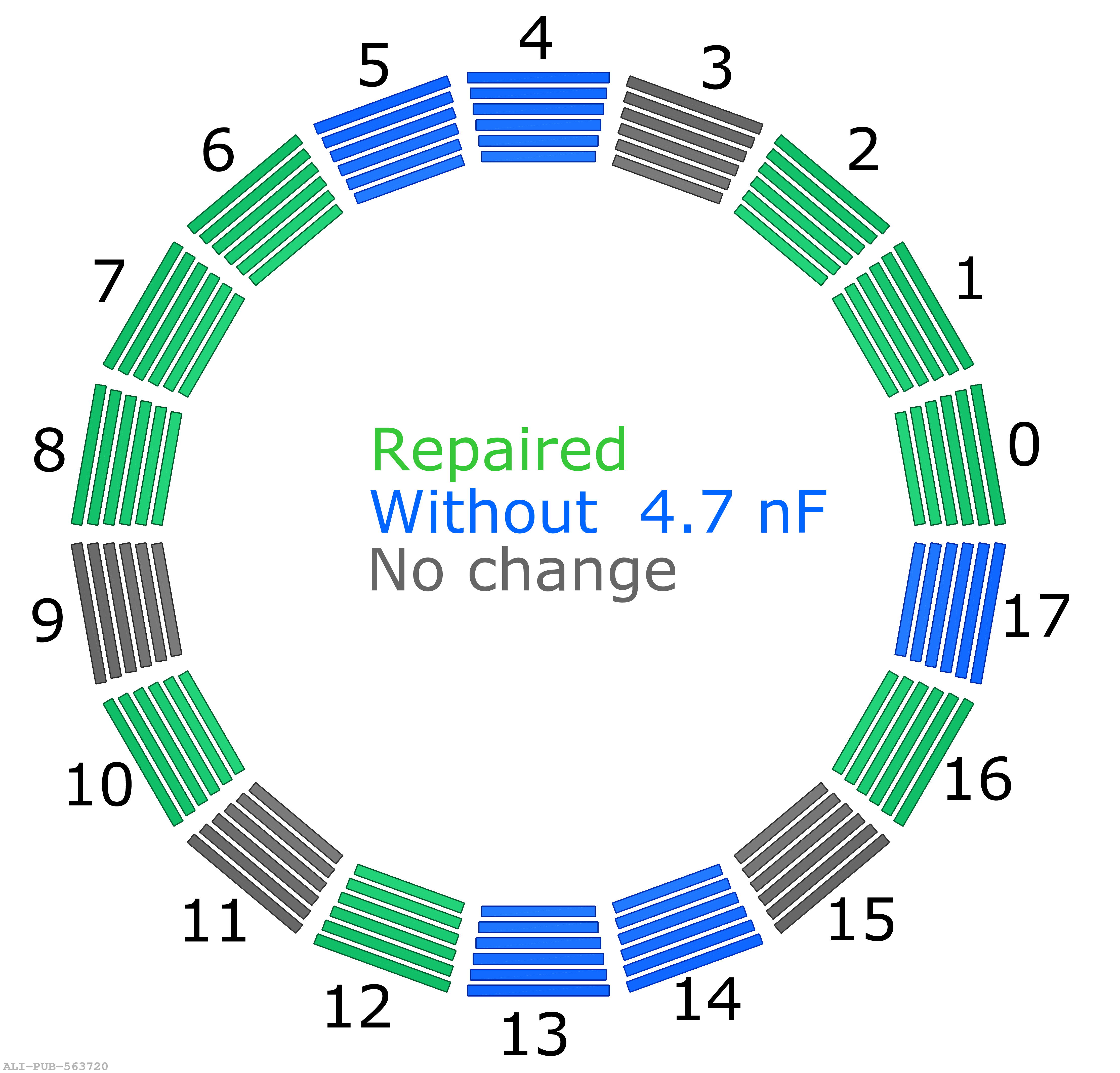
Figure 70
Induced common-mode signal with and without capacitors for the anode high-voltage. The baseline of pads in the same high-voltage segment as a cosmic-ray particle with an integrated signal between 10\,000 and 12\,500 ADC counts is shown before (red) and after (blue) the removal of the capacitors. For comparision, the baseline from pads in a high-voltage segment without hits is shown in green. | 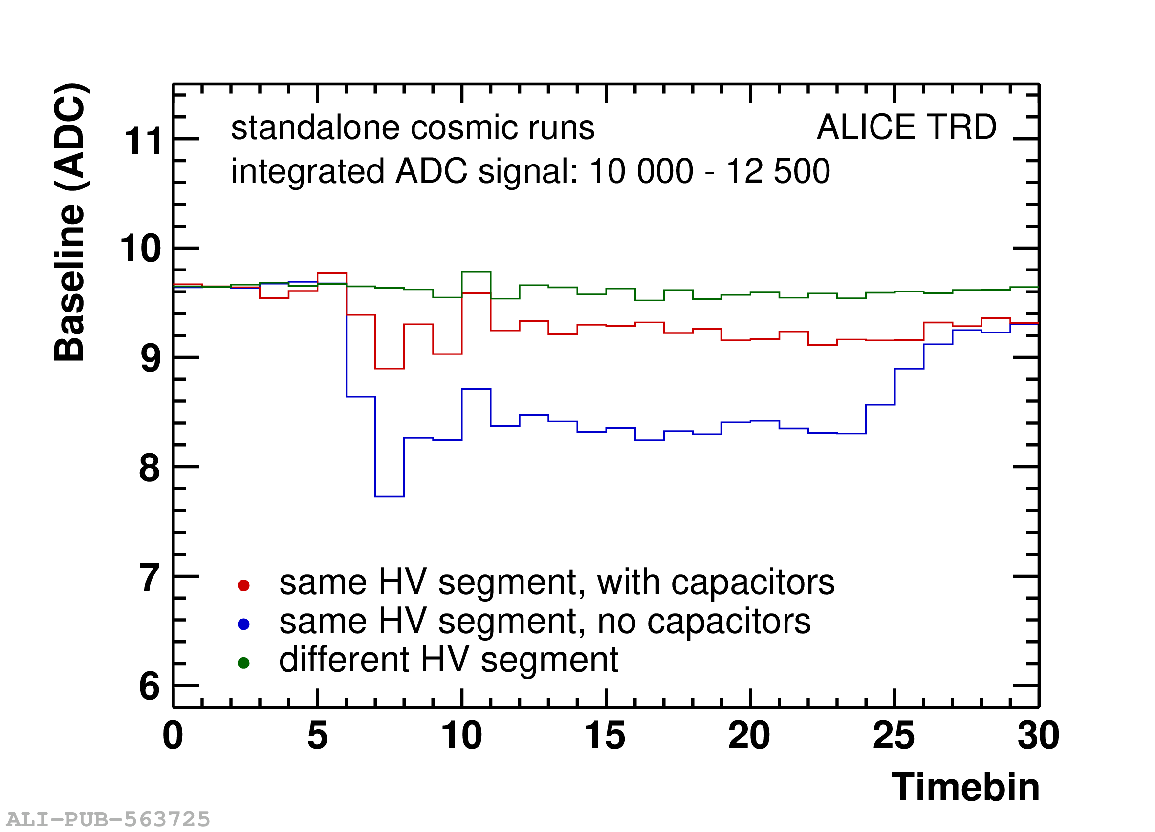 |
Figure 71
Left: $\Delta\alpha$ versus impact angle for a typical TRD chamber in Run 2, having a fixed uncalibrated drift velocity. The quoted values refer to the Run 2 calibration procedure (upper row) and to the new calibration scheme (lower row). Right: Average $\Delta\alpha$ versus impact angle for all TRD chambers after the calibration was applied. The red band shows the RMS of the distribution. | 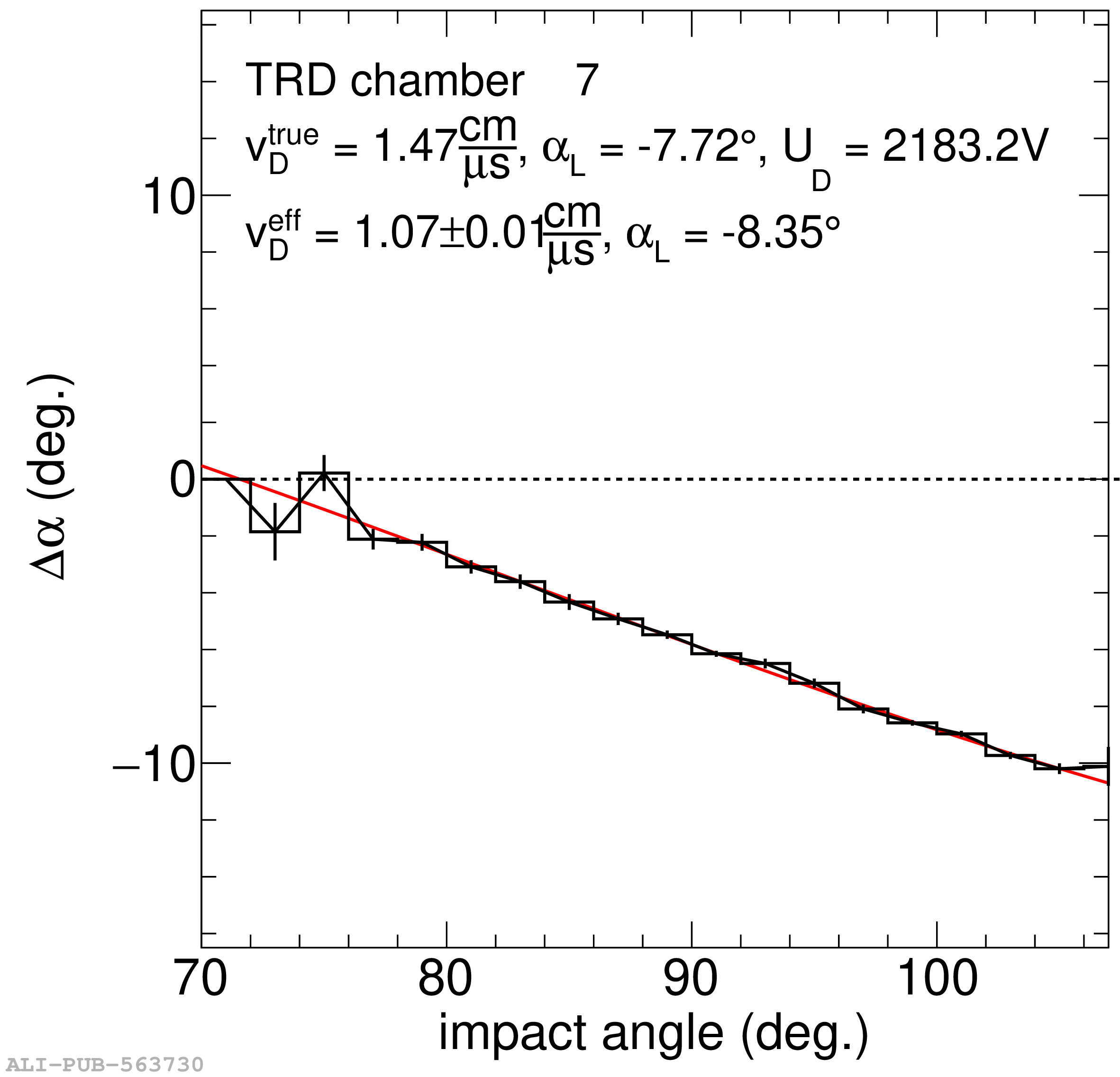 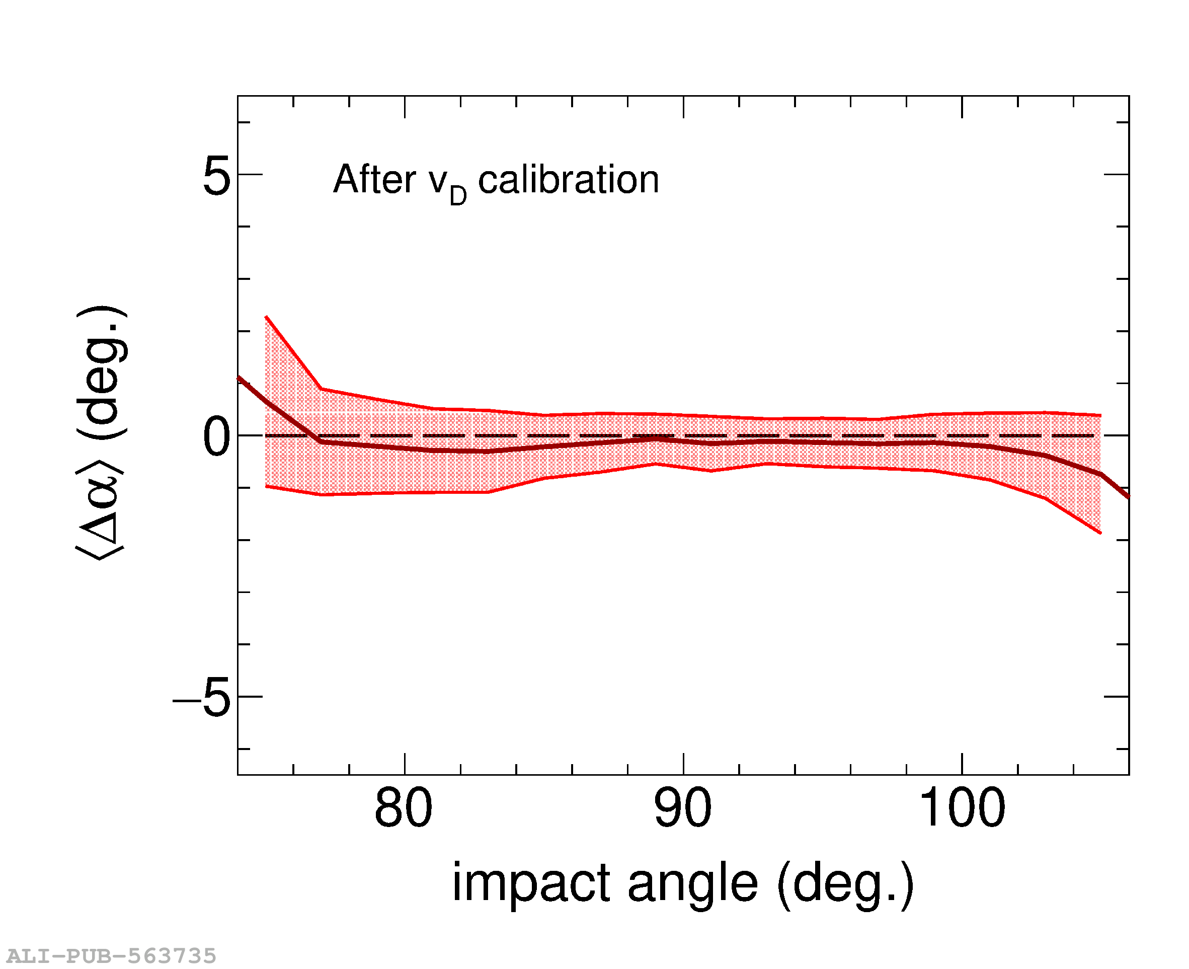 |
Figure 72
(left) HPTDC programming in Run 1 and 2 operations (top arrow) and in Run 3 (bottom arrow). The three trigger levels L0, L1 and L2a are replaced by a periodic trigger with a given frequency, mimicking a continuous readout. All hits (black lines) are read out and can be associated to physical events at a later stage. (right) Possible selection of parameters (fixed trigger frequency $f_\mathrm{T}$ and matching window width $m_\mathrm{w}$) to realize a continuous readout. The green circle corresponds to the chosen point of operations. | 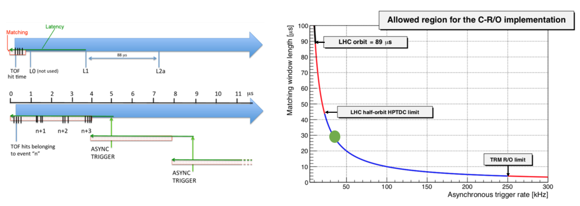 |
Figure 73
Hit time within the orbit of randomized hits sent at fixed rate to HPTDC inside a TOF crate operated in continuous readout mode. No holes are seen in the distribution, which means that random hits are received in all 3564 bunch crossings through the whole LHC orbit. | 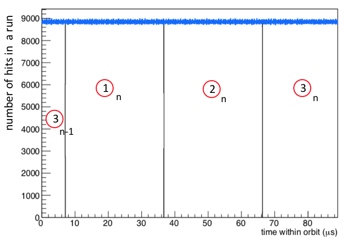 |
Figure 74
The DRM2 card: on the left the VTRX transceiver and the GBTx ASIC (covered by a heat dissipating panel). On the right the ARM piggy-back card is visible. The additional optical receivers for the SCL and the LHC clock are in the middle of the front panel. |  |
Figure 75
From left to right: HMPID Front-End Electronics (FEE), Readout Control Board (RCB) with the readout FPGA, the TTCRx and the Source Interface Unit (SIU). On the right, the C-RORC cards installed on O$^{2}$ FLP computers. |  |
Figure 76
HMPID full DAQ structure. Four C-RORC boards are installed on two First Level Processor (FLP) computers of the O$^2$ data acquisition environment. Fourteen optical links connect the 14 RCBs, two per RICH module. | 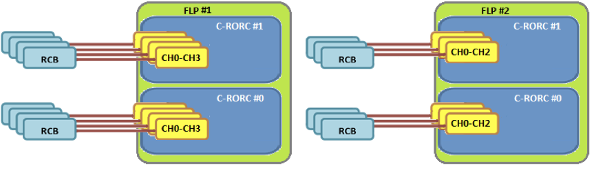 |
Figure 77
Event rate as a function of the detector occupancy, which is on average about 0.17\% and 2\% in \pp and \PbPb collisions, respectively. | 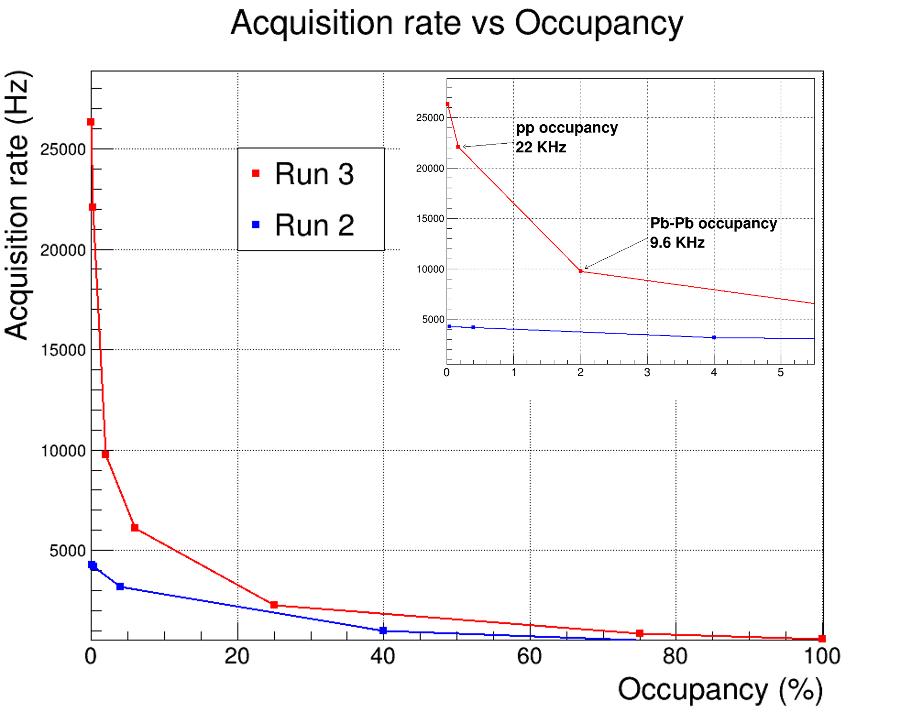 |
Figure 79
Schematic view of the EMCal, consisting of two disjunct detector segments, in the top-left hemisphere and the bottom-right hemisphere (DCal), covering approximately opposite locations in azimuth. The PHOS calorimeter inside the DCal segment is indicated in brown. | 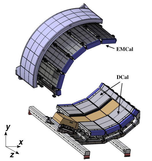 |


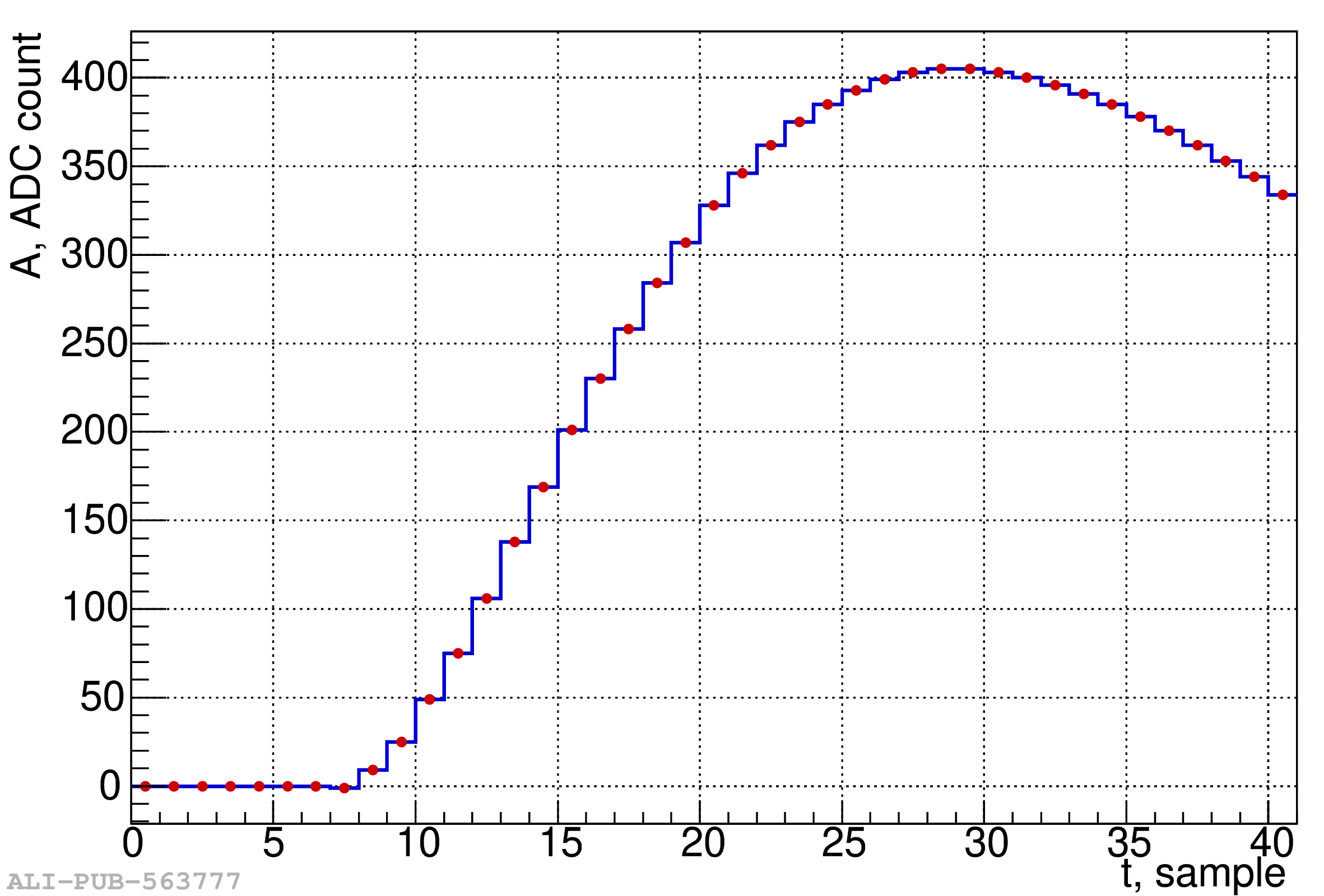

Figure 84
Performance of the digitizer during Pb--Pb 2018 data taking in the operating conditions chosen for Run 3. On the left plot: the lower part of the triggered spectrum of ZNC common photomultiplier in Pb--Pb collisions where the emission of a single $\SI{2.76}{\tera\electronvolt}$ neutron and multiples are visible. The spectrum is fitted to a superposition of gaussian functions whose peak positions $\mu_i$ are related to the neutron multiplicity by the relation $\mu_i=\mu_{1n}\times i$ and their widths by the relation $\sigma_{i}=\sigma_{1n}\sqrt{i}$, where $i$ is the neutron multiplicity and $\mu_{1n}$ and $\sigma_{1n}$ are the mean and the r.m.s. of the single neutron peak, respectively. The autotrigger algoritm effectively rejects pedestal events. On the right plot: the arrival time of ZNC common photomultiplier signals w.r.t. the reference ALICE L0 trigger signal. |   |
Figure 85
The cage: a support structure for beam pipe, ITS2, and MFT. Shown is the cage (magenta) with the bottom half of ITS and MFT as well as the beam pipe already installed. |  |
Figure 86
Beam pipe installed for the ALICE 2 detector with an outer diameter of \SI{36}{\mm}. | 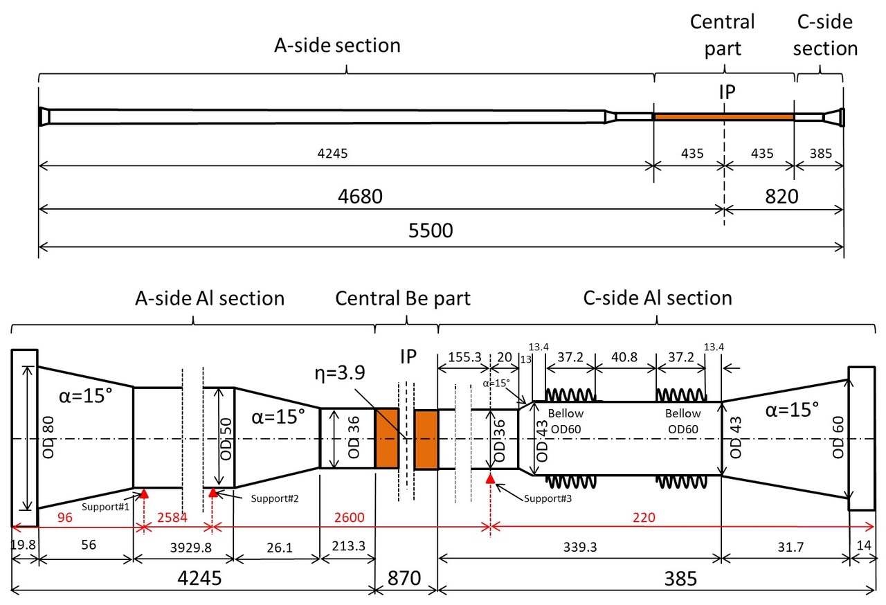 |
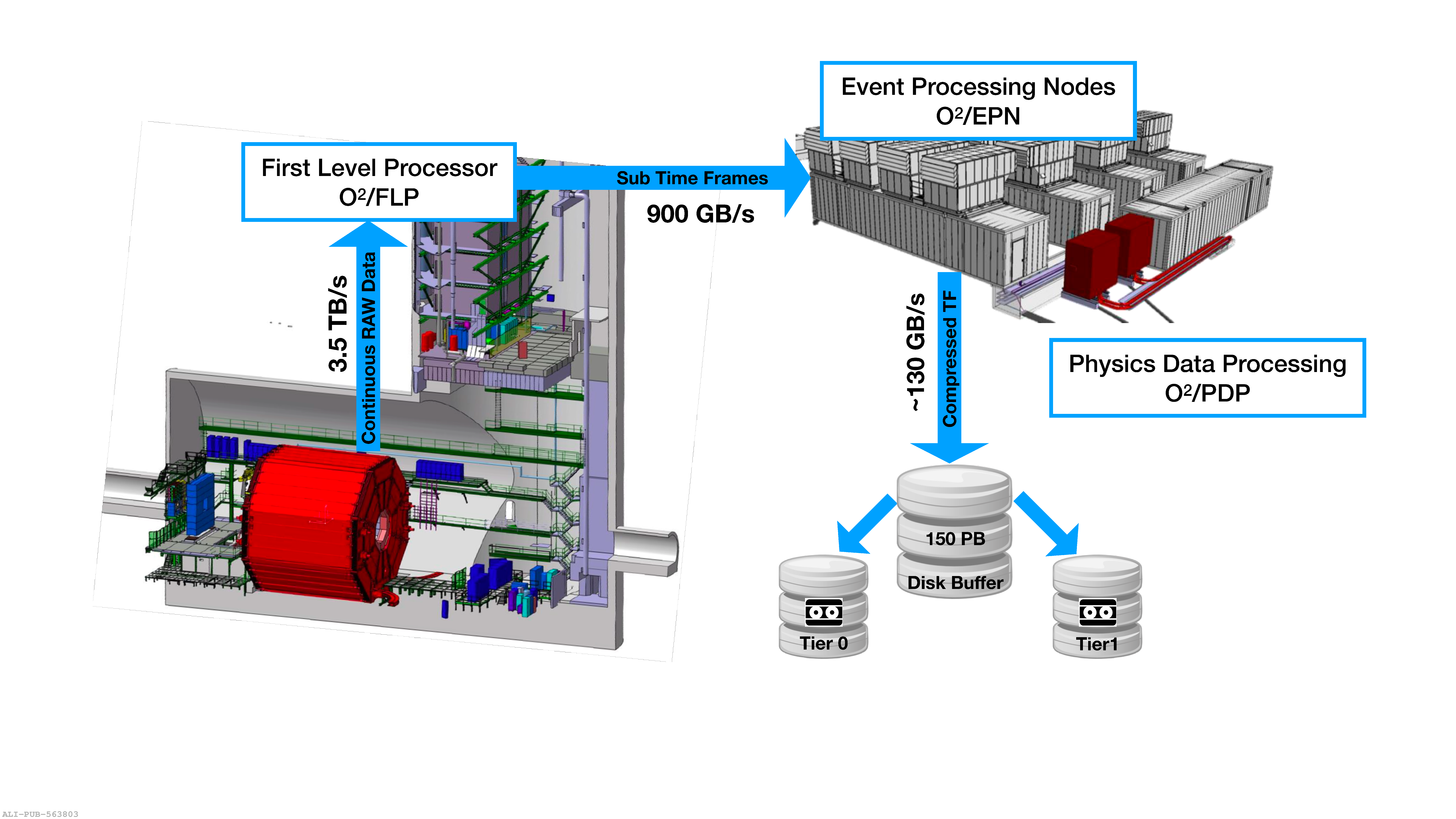
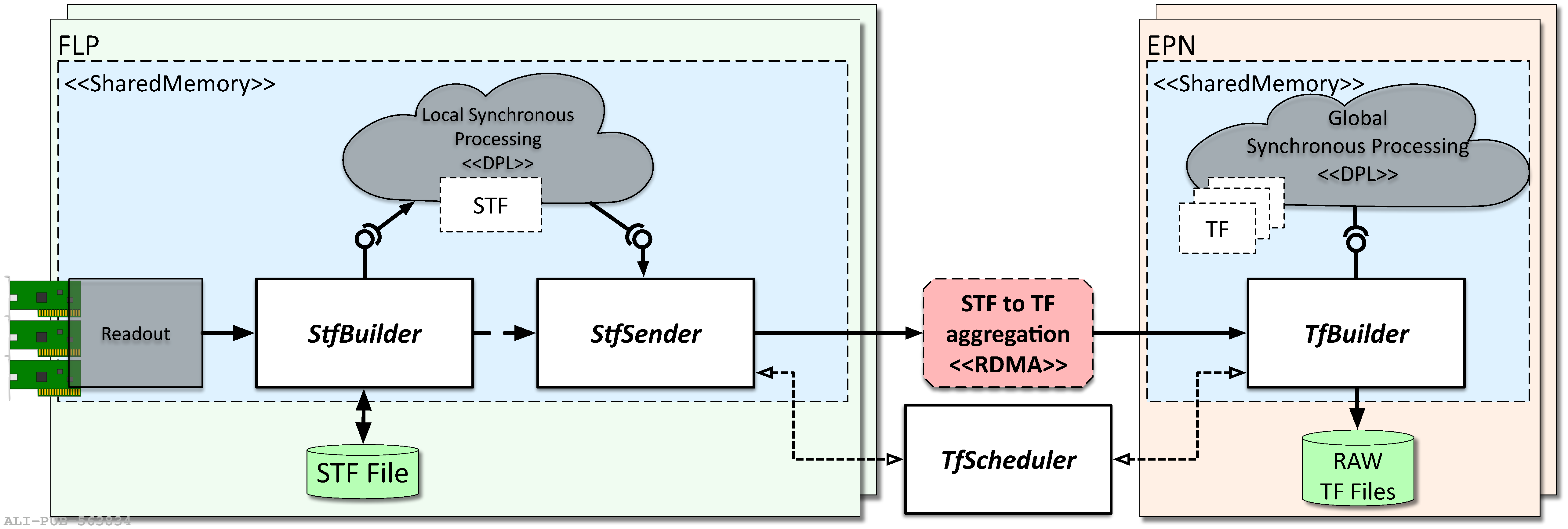
Figure 89
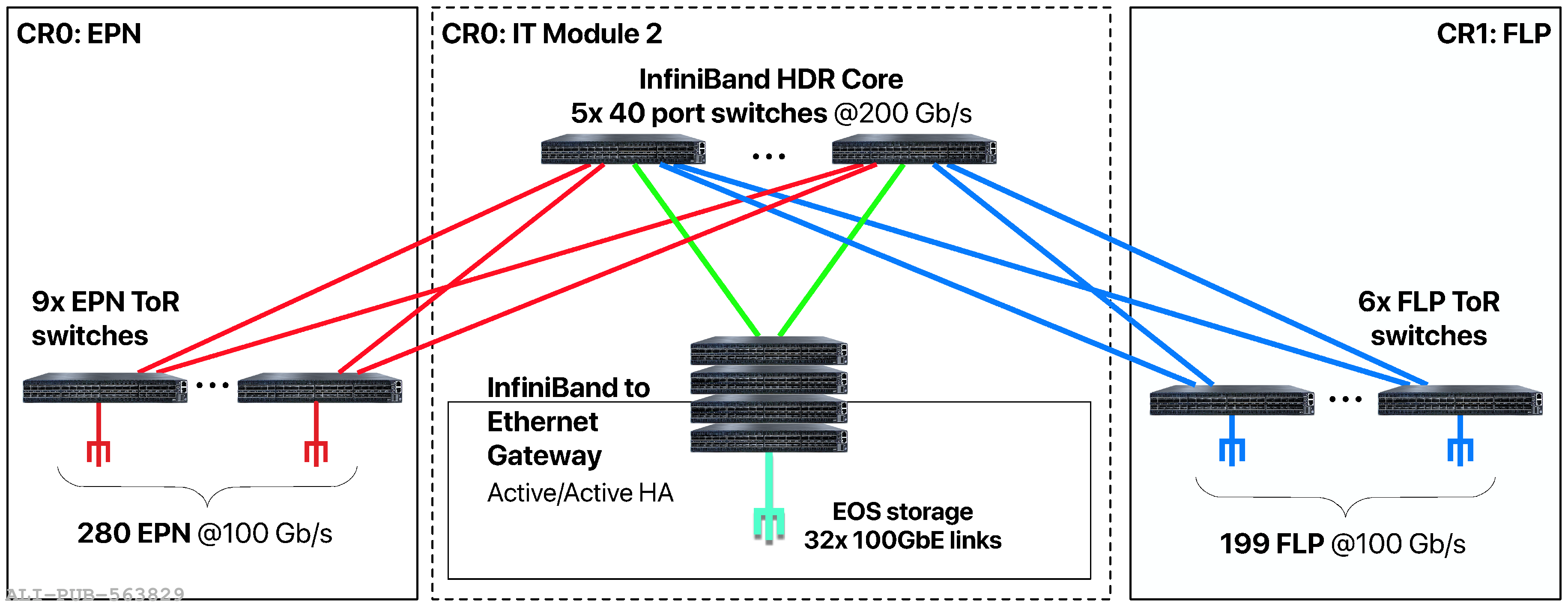
Simultaneous dataflows inside the FLP from the CRUs to the DDR memories and from the memory to the Infiniband network to the EPN farm. | 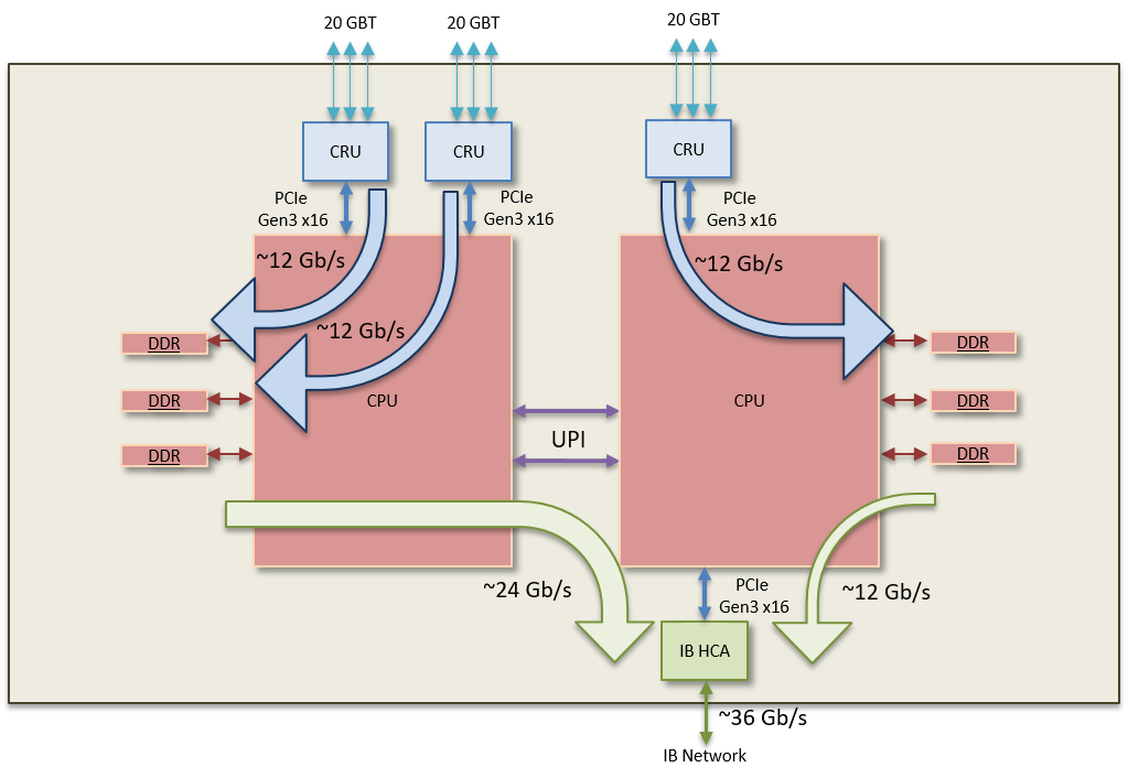 |